Architecture Innovations for the AI Era
Artilux composes its GeSi devices into system-level architectures — from high-speed optical interconnect to photonic computing — engineered for the bandwidth, latency, and energy demands of modern AI. Sensing, communication, and computing converge into a single photonic fabric.
Building the fabric of photonic intelligence
Together, Artilux’s fundational breakthroughs — spanning Halcyon™ photodetectors, Phoenix™ APDs, Nova™ SPADs, Metalens, and Ge EAM modulators — form a unified photonic foundation that merges sensitivity, speed, and scalability. These components are not isolated technologies but building blocks of an integrated photonic ecosystem, designed to communicate, sense, and compute using light.
By vertically integrating device, circuit, and system design within CMOS-compatible processes, Artilux transforms fundamental semiconductor innovation into system-level architectures that redefine how information is transmitted, processed, and understood — paving the way for the next era of photon-based intelligence.
Ultra-low-power analog computing, reinvented
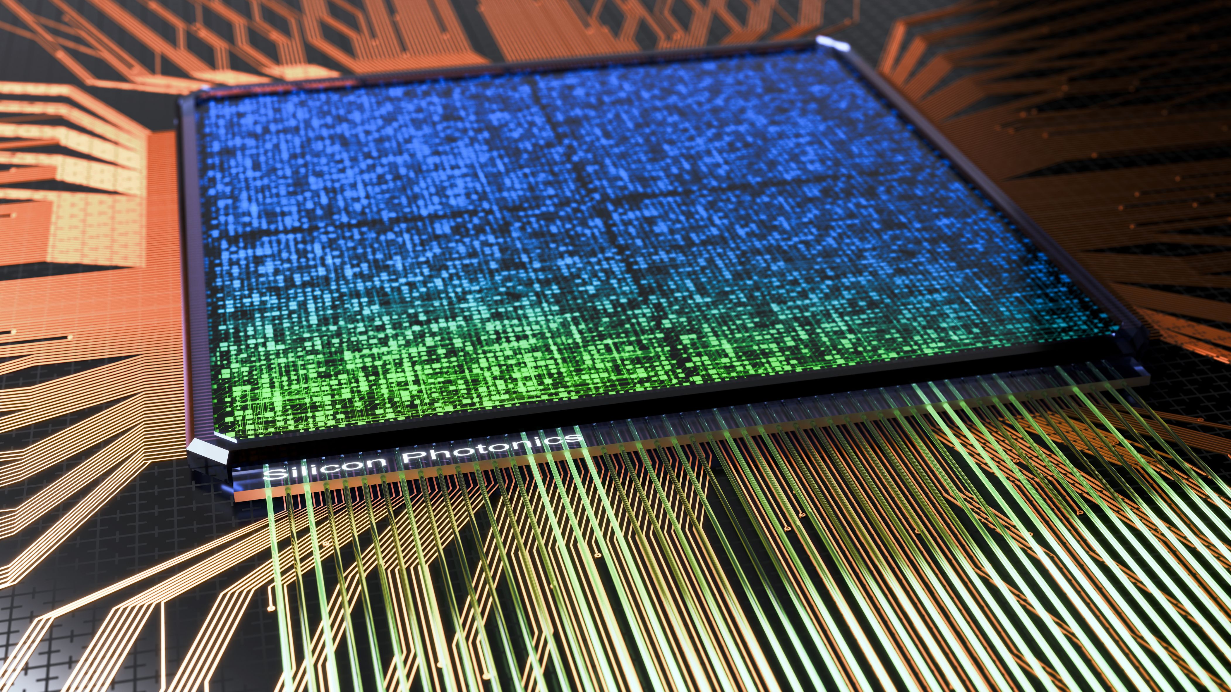
At Artilux, we are exploring the next frontier where light itself becomes the medium of computation. Building on our proprietary GeSi photonic platform, we are developing breakthrough architectures that harness the analog richness and parallelism of photons to perform computation with unprecedented speed and energy efficiency. While details remain under wraps, this initiative represents a bold step toward a future where sensing, communication, and computing converge into a unified photonic fabric — transforming how intelligence is generated, transmitted, and perceived.
Learn more about photonic computing →Cryogenics-Free Quantum Computing: Room-Temperature Integrated Photonics Powered by GeSi SPADs
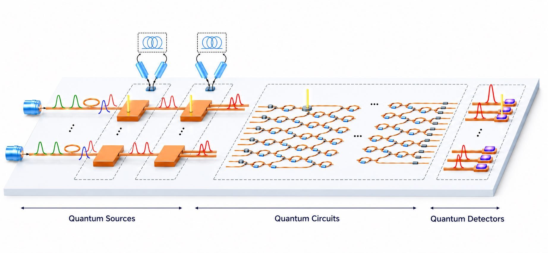
Artilux has proposed a room-temperature photonic quantum computing architecture built on integrated silicon photonics and germanium–silicon single-photon avalanche diodes (GeSi SPADs). Unlike traditional platforms that require bulky cryogenic cooling, this approach replaces cryo-detectors with waveguide-integrated GeSi SPADs operating at 260K-300K. The fully integrated chip combines on-chip photon quantum sources using active temporal multiplexing, a programmable interferometer circuit mesh for executing algorithms, and spatially multiplexed GeSi SPAD detectors that enable photon-number resolution at room temperature. Built on standard silicon-on-insulator and germanium-on-silicon platforms, this architecture is fully CMOS-compatible and supports hybrid ASIC integration—delivering a scalable path to mass-deployable, cryogenics-free quantum computing.
Core Architecture Components
The architecture, illustrated above, divides full PQC integration into three main functional blocks:
1. Quantum Sources: On-chip spontaneous four-wave mixing (SFWM) sources generate single-photon pairs using silicon-on-insulator (SOI) ring resonators, followed by active temporal multiplexing to deliver high-purity single photons.
2. Quantum Circuits: A field-programmable interferometer mesh (FPIM) consisting of cascaded Mach–Zehnder interferometers (MZIs) performs target quantum algorithms by routing photons along distinct paths.
3. Quantum Detectors: Waveguide-integrated GeSi SPADs operate at room temperature. By arranging these detectors in a spatially multiplexed M-fold waveguide array, the setup acts as a photon-number-resolving avalanche diode (PNRAD) to resolve multi-photon states.
Learn more about photonic quantum computing →Architect the
photonic fabric
Artilux builds integrated GeSi photonic architectures — from fast waveguide links to wide array fabrics and photonic computing — enabling AI systems to run on light.